
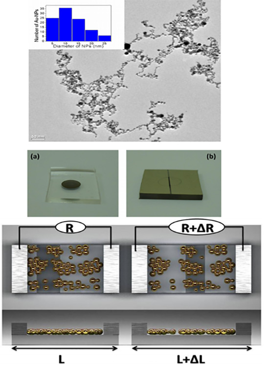
We demonstrate high strain sensitivity property of gold nanoparticle (Au-NP) thin films fabricated on flexible polydimethylsiloxane (PDMS) substrates. This behavior is attributed to quantum tunneling effect that is highly dependent on nanoparticle separation. Au-NPs were synthesized in water by nanosecond laser ablation method. The clean surface providing high tunneling decay constant, size of the Au-NPs and Au-NPs aggregate clusters offer advantages for high sensitivity strain sensor. We prepared Au-NPs films on flexible PDMS substrate by using hands-on drop-cast method. To obtain high gauge factor (g factor), we investigated the nanoparticles concentration on the substrate. Laser-generated Au-NPs films demonstrated g factor of ∼300 for higher than 0.22% strain and ∼80 for the strain lower than 0.22% strain, which is favorably comparable to reported sensitivities for strain sensors based on Au-NPs. Mechanical characterizations for the prolonged working durations suggest long term stability of the strain sensors. We discuss several models describing conductance of films in low and high strain regimes.
Laser synthesized gold nanoparticles for high sensitive strain gauges
S. Burzhuev, A. Dana and B. Ortaç Sensors & Actuators: A. Physical, vol. 203, pp. 131-136 (2013)
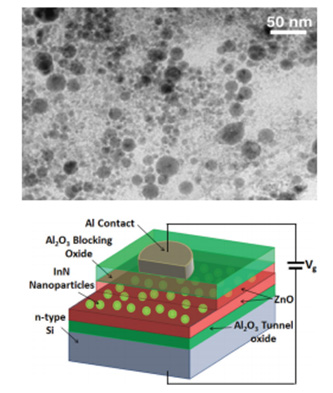
In this work, the fabrication of charge trapping memory cells with laser-synthesized indium-nitride nanoparticles (InN-NPs) embedded in ZnO charge trapping layer is demonstrated. Atomic layer deposited Al2O3 layers are used as tunnel and blocking oxides. The gate contacts are sputtered using a shadow mask which eliminates the need for any lithography steps. High frequency C-Vgate measurements show that a memory effect is observed, due to the charging of the InN-NPs. With a low operating voltage of 4 V, the memory shows a noticeable threshold voltage (Vt) shift of 2 V, which indicates that InN-NPs act as charge trapping centers. Without InN-NPs, the observed memory hysteresis is negligible. At higher programming voltages of 10 V, a memory window of 5 V is achieved and the Vt shift direction indicates that electrons tunnel from channel to charge storage layer.
Enhanced memory effect via quantum confinement in 16 nm InN nanoparticles embedded in ZnO charge trapping layer
N. El-Atab, F. Cimen, S. Alkis, B. Ortaç, M. Alevli, N. Dietz, A. K. Okyay and A. Nayfeh Applied Physics Letters, vol. 104, , pp. 253106-261105-4 (2014)
We present a proof-of-concept photodetector that is sensitive in the near-infrared (NIR) range based on InN nanocrystals. Indium nitride nanocrystals (InN-NCs) are obtained through laser ablation of a high pressure chemical vapor deposition grown indium nitride thin film and are used as optically active absorption region. InN-NCs are sandwiched between thin insulating films to reduce the electrical leakage current. Under −1 V applied bias, the recorded photoresponsivity values within 600–1100-nm wavelength range are as high as 3.05 × 10⁻² mA/W. An ultrathin layer of nanocrystalline InN thin film is, therefore, a promising candidate for NIR detection in large area schemes.

A near-infrared range photodetector based on indium nitride nanocrystals obtained through laser ablation
B. Tekcan, S. Alkis, M. Alevli, N. Dietz, B. Ortaç, N. Biyikli and A. K. Okyay IEEE Electron Device Letters, vol. 35, pp. 936-938 (2014)
We report on the development of UV range photodetector based on molybdenum disulfide nanocrystals (MoS2-NCs). The inorganic MoS2- NCs are produced by pulsed laser ablation technique in deionized water and the colloidal MoS2-NCs are characterized by transmission electron microscopy, Raman spectroscopy, X-ray diffraction and UV/VIS absorption measurements. The photoresponse studies indicate that the fabricated MoS2- NCs photodetector (MoS2-NCs PD) operates well within 300-400 nm UV range, with diminishing response at visible wavelengths, due to the MoS2- NCs absorption characteristics. The structural and the optical properties of laser generated MoS2-NCs suggest promising applications in the field of photonics and optoelectronics.

Thin film MoS2 nanocrystal based ultraviolet photodetector
S. Alkis, T. Öztaş, L. E. Aygün, F. Bozkurt, A. K. Okyay and B. Ortaç Optics Express, vol. 20, pp. 21815-21820 (2012)
We present a proof-of-concept photodetector which is sensitive in the visible spectrum. Silicon nanocrystals (Si-NCs) obtained by laser ablation are used as the active absorption region. Si-NC films are formed from a polymeric dispersion. The films are sandwiched between thin insulating films to reduce the electrical leakage current. Furthermore, Ag nanoparticles are integrated with the photodetector to enhance the visible response using plasmonic effects. The measured photocurrent is resonantly enhanced, which is explained in terms of enhanced local fields caused by localized plasmons. The UV–vis spectrum of Ag nanoparticles is also measured to verify the resonance.

Plasmonic Enhanced Photodetector Based on Silicon Nanocrystals Obtained Through Laser Ablation
S. Alkis, F. B. Oruç, B. Ortaç, A. C. Koşger and A. K. Okyay Journal of Optics, vol. 14, pp. 125001 (2012)